- 您现在的位置:买卖IC网 > Sheet目录3881 > PIC18F8720T-E/PT (Microchip Technology)IC PIC MCU FLASH 64KX16 80TQFP
PIC18F6520/8520/6620/8620/6720/8720
DS39609B-page 120
2004 Microchip Technology Inc.
10.7
PORTG, TRISG and LATG
Registers
PORTG is a 5-bit wide, bidirectional port. The corre-
sponding data direction register is TRISG. Setting a
TRISG bit (= 1) will make the corresponding PORTG
pin an input (i.e., put the corresponding output driver in
a high-impedance mode). Clearing a TRISG bit (= 0)
will make the corresponding PORTC pin an output (i.e.,
put the contents of the output latch on the selected pin).
The Data Latch register (LATG) is also memory
mapped. Read-modify-write operations on the LATG
register, read and write the latched output value for
PORTG.
PORTG is multiplexed with both CCP and USART
functions (Table 10-13). PORTG pins have Schmitt
Trigger input buffers.
When enabling peripheral functions, care should be
taken in defining TRIS bits for each PORTG pin. Some
peripherals override the TRIS bit to make a pin an
output, while other peripherals override the TRIS bit to
make a pin an input. The user should refer to the
corresponding peripheral section for the correct TRIS
bit settings.
The pin override value is not loaded into the TRIS reg-
ister. This allows read-modify-write of the TRIS register,
without concern due to peripheral overrides.
EXAMPLE 10-7:
INITIALIZING PORTG
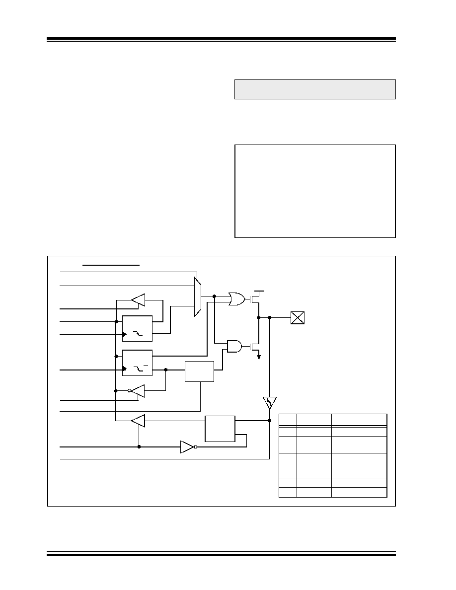
FIGURE 10-16:
PORTG BLOCK DIAGRAM (PERIPHERAL OUTPUT OVERRIDE)
Note:
On a Power-on Reset, these pins are
configured as digital inputs.
CLRF
PORTG
; Initialize PORTG by
; clearing output
; data latches
CLRF
LATG
; Alternate method
; to clear output
; data latches
MOVLW
0x04
; Value used to
; initialize data
; direction
MOVWF
TRISG
; Set RG1:RG0 as outputs
; RG2 as input
; RG4:RG3 as inputs
PORTG/Peripheral Out Select
Data Bus
WR LATG
WR TRISG
Data
Latch
TRIS Latch
RD TRISG
Q
D
Q
CK
QD
EN
Peripheral Data Out
0
1
Q
D
Q
CK
P
N
VDD
VSS
RD PORTG
Peripheral Data In
I/O pin(1)
or
WR PORTG
RD LATG
Schmitt
Trigger
Note 1:
I/O pins have diode protection to VDD and VSS.
2: Peripheral Output Enable is only active if Peripheral Select is active.
TRIS
Override
Peripheral Output
Logic
TRIS OVERRIDE
Pin
Override
Peripheral
RG0
Yes
CCP3 I/O
RG1
Yes
USART1 Async
Xmit, Sync Clock
RG2
Yes
USART1 Async
Rcv, Sync Data
Out
RG3
Yes
CCP4 I/O
RG4
Yes
CCP5 I/O
Enable(2)
发布紧急采购,3分钟左右您将得到回复。
相关PDF资料
PIC18F4439T-E/ML
IC PIC MCU FLASH 6KX16 44QFN
XF2J-2824-11
CONN FPC 28POS 0.5MM SMT
PIC18F4439T-E/PT
IC PIC MCU FLASH 6KX16 44TQFP
PIC18F6585T-I/PT
IC PIC MCU FLASH 24KX16 64TQFP
PIC18LF8525T-I/PT
IC PIC MCU FLASH 24KX16 80TQFP
PIC18F6720T-E/PT
IC PIC MCU FLASH 64KX16 64TQFP
PIC18F4539T-E/PT
IC PIC MCU FLASH 12KX16 44TQFP
PIC16F685-I/P
IC PIC MCU FLASH 4KX14 20DIP
相关代理商/技术参数
PIC18F8720T-I/PT
功能描述:8位微控制器 -MCU 128KB 3840 RAM 68I/O RoHS:否 制造商:Silicon Labs 核心:8051 处理器系列:C8051F39x 数据总线宽度:8 bit 最大时钟频率:50 MHz 程序存储器大小:16 KB 数据 RAM 大小:1 KB 片上 ADC:Yes 工作电源电压:1.8 V to 3.6 V 工作温度范围:- 40 C to + 105 C 封装 / 箱体:QFN-20 安装风格:SMD/SMT
PIC18F8721-I/PT
功能描述:8位微控制器 -MCU 128kBF 4096RM 40MHz nonoWatt RoHS:否 制造商:Silicon Labs 核心:8051 处理器系列:C8051F39x 数据总线宽度:8 bit 最大时钟频率:50 MHz 程序存储器大小:16 KB 数据 RAM 大小:1 KB 片上 ADC:Yes 工作电源电压:1.8 V to 3.6 V 工作温度范围:- 40 C to + 105 C 封装 / 箱体:QFN-20 安装风格:SMD/SMT
PIC18F8721T-I/PT
功能描述:8位微控制器 -MCU 128kBF 4096RM 40MHz nonoWatt RoHS:否 制造商:Silicon Labs 核心:8051 处理器系列:C8051F39x 数据总线宽度:8 bit 最大时钟频率:50 MHz 程序存储器大小:16 KB 数据 RAM 大小:1 KB 片上 ADC:Yes 工作电源电压:1.8 V to 3.6 V 工作温度范围:- 40 C to + 105 C 封装 / 箱体:QFN-20 安装风格:SMD/SMT
PIC18F8722 DEVELOPMENT BOARD KIT
功能描述:DEVELOPMENT BOARD FOR PIC18F8722 RoHS:否 类别:编程器,开发系统 >> 通用嵌入式开发板和套件(MCU、DSP、FPGA、CPLD等) 系列:- 标准包装:1 系列:PICDEM™ 类型:MCU 适用于相关产品:PIC10F206,PIC16F690,PIC16F819 所含物品:板,线缆,元件,CD,PICkit 编程器 产品目录页面:659 (CN2011-ZH PDF)
PIC18F8722 DEVELOPMENT KIT
功能描述:EMBEDDED C DEVELOPMENT KIT RoHS:否 类别:编程器,开发系统 >> 通用嵌入式开发板和套件(MCU、DSP、FPGA、CPLD等) 系列:PIC® 产品培训模块:Blackfin® Processor Core Architecture Overview
Blackfin® Device Drivers
Blackfin® Optimizations for Performance and Power Consumption
Blackfin® System Services 特色产品:Blackfin? BF50x Series Processors 标准包装:1 系列:Blackfin® 类型:DSP 适用于相关产品:ADSP-BF548 所含物品:板,软件,4x4 键盘,光学拨轮,QVGA 触摸屏 LCD 和 40G 硬盘 配用:ADZS-BFBLUET-EZEXT-ND - EZ-EXTENDER DAUGHTERBOARDADZS-BFLLCD-EZEXT-ND - BOARD EXT LANDSCAP LCD INTERFACE 相关产品:ADSP-BF542BBCZ-4A-ND - IC DSP 16BIT 400MHZ 400CSBGAADSP-BF544MBBCZ-5M-ND - IC DSP 16BIT 533MHZ MDDR 400CBGAADSP-BF542MBBCZ-5M-ND - IC DSP 16BIT 533MHZ MDDR 400CBGAADSP-BF542KBCZ-6A-ND - IC DSP 16BIT 600MHZ 400CSBGAADSP-BF547MBBCZ-5M-ND - IC DSP 16BIT 533MHZ MDDR 400CBGAADSP-BF548BBCZ-5A-ND - IC DSP 16BIT 533MHZ 400CSBGAADSP-BF547BBCZ-5A-ND - IC DSP 16BIT 533MHZ 400CSBGAADSP-BF544BBCZ-5A-ND - IC DSP 16BIT 533MHZ 400CSBGAADSP-BF542BBCZ-5A-ND - IC DSP 16BIT 533MHZ 400CSBGA
PIC18F8722-E/PT
功能描述:8位微控制器 -MCU 128 KB FL 3936 RAM 25 MHz RoHS:否 制造商:Silicon Labs 核心:8051 处理器系列:C8051F39x 数据总线宽度:8 bit 最大时钟频率:50 MHz 程序存储器大小:16 KB 数据 RAM 大小:1 KB 片上 ADC:Yes 工作电源电压:1.8 V to 3.6 V 工作温度范围:- 40 C to + 105 C 封装 / 箱体:QFN-20 安装风格:SMD/SMT
PIC18F8722-I/PT
功能描述:8位微控制器 -MCU 128 KB FL 4K RAM 70 I/O RoHS:否 制造商:Silicon Labs 核心:8051 处理器系列:C8051F39x 数据总线宽度:8 bit 最大时钟频率:50 MHz 程序存储器大小:16 KB 数据 RAM 大小:1 KB 片上 ADC:Yes 工作电源电压:1.8 V to 3.6 V 工作温度范围:- 40 C to + 105 C 封装 / 箱体:QFN-20 安装风格:SMD/SMT
PIC18F8722T-E/PT
功能描述:8位微控制器 -MCU 128 KB FL 3936 RAM 25MHz RoHS:否 制造商:Silicon Labs 核心:8051 处理器系列:C8051F39x 数据总线宽度:8 bit 最大时钟频率:50 MHz 程序存储器大小:16 KB 数据 RAM 大小:1 KB 片上 ADC:Yes 工作电源电压:1.8 V to 3.6 V 工作温度范围:- 40 C to + 105 C 封装 / 箱体:QFN-20 安装风格:SMD/SMT